SiC-based hydrocarbons sensors for security in hostile industrial environments
Hydrocarbon sensors based on silicon carbide (SiC) unipolar devices will be designed, fabricated and tested in hostile environments. Using SiC, a wide-bandgap semiconductor with excellent tolerance to high temperatures, chemical agents and radiation, enables the development of technologies for reliable electronic devices, intended for hydrocarbon concentration monitoring in hostile industrial applications.
In order to reach the projects objectives, considering existing limitations reported in literature, novel solutions will be implemented for fabricating the sensor structure as well as design and execution of high-performing circuits for sensor output signal processing. The sensor system will be tested in real working conditions, at the Fieni cement factory.
UPB is in charge of the gas sensor structure design, development of the acquisition and conversion circuits (CEAS/CONVI), as well as the implementation of the system for measurement and characterization with temperature of SiC sensors.
IMT develops the fabrication technology, manufacture the gas sensor structures, implement technological methods of catalytic metal nano-structuring and participate in testing and characterization.
1.Integrated hydrocarbon sensor system. Experimental model
The ”Smart” sensor denomination is justified by implementing an integrated system comprising a SiC MOS capacitor (the sensor itself) and circuitry specialized in signal acquisition, processing and analog/digital conversion (CEAS/CONVI) – Fig. 1.
The proposed system comprises an analog module (PLL-based measurement circuit – CEAS) and a digital module, for signal acquisition, processing and user interfacing (CONVI). The analog module (CEAS) has a DPLL (Digital PLL) structure and contains two voltage controlled oscillators (VCOs), a digital phase and frequency detector and a low-pass filter. The frequencies of the signals outputted by the two VCOs are given by two sensors: a reference (insensitive to gas) and the active sensor. These frequencies are tuned by the digital phase and frequency detector through a control voltage, which is proportional to the gas concentration. The measurement is differential, which eliminates parasitic influences such as temperature variations. The conversion module (CONVI) is digital at this stage and is used to control the PLL and process its output signal. It is made up of a microcontroller and A/D – D/A converters. The data is displayed via an LCD.
2.Design of SiC device fabrication technology. Design and implementation of photolithographic masks
The variable-capacity SiC devices were fabricated starting from 4H-SiC wafers with two epitaxial layers: a 0.5 µm buffer with 1018 cm-3 doping and an active layer with a thickness up to 10 µm and 1016 cm-3 doping. The final version of the photolithographic masks for fabricating these devices is given in Fig. 2.
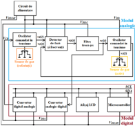
Fig. 1 a) Block schematic of the CEAS/CONVI system.
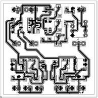
Fig. 1 -b) CEAS Layout.
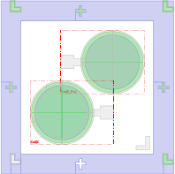
Fig. 2 Structure of variable capacity SiC devices.
Stage 2, carried out in 2019, titled Hydrocarbon sensing integrated system. Experimental model, presents the fabrication and packaging of VARICAP devices which will be used as gas sensors. Characterization and laboratory testing of sensing structures were performed with a dedicated measurement and electrical characterization system with temperature. All projected activities in the workplan were implemented as follows:
2.2.1 Fabrication of VARICAP device batches. Microphysical investigations.
The VARICAP devices are SiC-based MOS capacitors, fabricated starting from a 4H-SiC wafer with a bulk-doping of approx. 1018 cm-3 and epitaxial layer doping of about 2·1016 cm-3. After a standard chemical cleaning process, a 600 nm SiO2 film was deposited on the epitaxial layer for passivation. The active areas of the MOS capacitors were defined by etching circular windows in the oxide. A thin oxide layer (the MOS oxide) was thermally grown inside these windows at 1100°C for 2.5 h, in dry O2 atmosphere. A thickness of approx. 30 nm was determined from standard electrical measurements. Microphysical characterization of the MOS SiC sensor structures (using XRD, etc) was primarily focused on determining the properties of the MOS oxide. The oxide/SiC interface was also investigated. An interface layer thickness of approx. 2.8 nm was determined, with the profile given in Fig. 2.1.1.
As can be observed, an oxide density of 2.12 g/cm3 was obtained. The C concentration (resulting from carbonic compounds) at the SiO2/SiC interface was also determined. It is evinced that the interface layer becomes more carbon-rich in the vicinity of the semiconductor (the SiC substrate).
After MOS oxide growth, 50 nm of Ni were deposited on the wafer backside for ohmic contacting. The process was followed by a rapid thermal annealing at 400°C, for 5 min. in Ar atmosphere.
A thin layer of Pd (50 nm) was deposited on the MOS oxide in order to obtain the gate electrode. The electrode’s area is larger than the active window’s (450 μm in diameter, a 50 μm increase), which ensures the complete contacting of the active area and facilitates obtaining the pads on the protection oxide. Thus, the entire active area can be exposed to gas molecules when the VARICAP structure operates as a gas hydrocarbon sensor. Pd was chosen due to its exemplary solubility in hydrogen.
Finally, the individual MOS capacitor structures were diced and prepared for electrical measurements and characterization (min. 50 VARICAP structures – physical objects).
2.2.2 Ambase bonding techniques for the SiC devices. Packaging of SiC-sensor structures.
Packaging is an essential process for obtaining high-temperature capable sensors. The altering of sensing parameters during operation at over 200°C is owed, in most practical application, to the degradation of capsule and its terminals. In order to achieve a reliable packaging process, multiple metallic capsules with glass-based terminal/body insulation were investigated. The capsules were subjected to 1000 50°C-400°C thermal cycles. Following the tests, the TO39 capsule was selected, due to the superior performances of its gold-plated ambase and terminals. The packaging technology for sensor structures was established. The anode is contacted to the ambase’s insulated terminal via a 25 µm thick gold wire. The cathode is connected directly to the ambase. Multiple bonding techniques were tested for this procedure, such as using Au or Ag-based thermal and electrical conductive paste, Au-In preform, or solid-solid diffusion.
An investigated solid-solid diffusion technique for the SiC VARICAP structures (physical objects) used an Ag nano-particle layer. Due to the size of the nano-particles, the equivalent chip-ambase pressure increases by several orders of magnitude, significantly reducing the temperature-time budget required for bonding.
2.2.3 Design and implementation of a SiC gas sensor electrical measurement and characterization system with temperature. Sensor parameter extraction.
Sensor characterization and testing requires measuring C-V characteristics as a function of gas concentration. A study of literature and preliminary measurements showed that the C-V characteristics are not only dependent on gas concentration but also on ambient temperature. Consequently, adequate characterization of gas sensors imposes the development of a measurement environment where these quantities can be precisely controlled. Thus, a testing system (physical object) was conceived and developed, with the block schematic in Fig. 2.3.1.
As can be seen in Fig. 2.3.1, the system comprises two complex installations:
Both equipments are controllable locally on their consoles, as well as remotely, from a PC, using the Ethernet interface. Thus, the system shows a high degree of flexibility and automation.
A study of sensor parameter extraction techniques was carried out, leading to the development of extraction software (computer product), implemented in LabVIEW 2010. The program uses C-V characteristics measured on the SiC VARICAP structures and first determines the oxide capacitance value (Cox) from the accumulation region. From the representation as a function of V, a linear fitting yields the epitaxial layer doping (ND, from the slope) and the flatband voltage (VFB from the intercept). Finally, the program calculates the threshold voltage (VT), which delimits the inversion and depletion regions. Using Cox values, the gate oxide thickness is determined (xox).
2.2.4 Characterization and laboratory testing of VARICAP SiC sensor devices (wafer and packaged device measurements)
The testing of VARICAP devices using the system in section 2.2.3 is performed according to the following procedure. Initially, the structures are placed in the gas enclosure (with controlled H2 concentration – Fig. 2.3.1). The enclosure is then inserted into the thermostat oven and connected to the semiconductor analyzer via ceramic crossings. Gas concentrations and temperature levels are set using the chromatograph’s control software. To minimize errors given by thermal inertia, temperature is monitored by two separate thermometers (the chromatograph’s internal thermometer and an external one) and measurements are performed when their indications are similar and stable.
The electrical parameters required for acquiring the C-V characteristics (voltage variation limits, frequency and amplitude of the AC component, etc.) are set through the semiconductor analyzer.
As mentioned previously, the gas sensors are SiC MOS capacitors, fabricated using the technology described in section 2.2.1. These VARICAP devices were electrically studied by measuring their C-V characteristics (see the above procedure) on wafer and packaged devices (study). Fig. 2.4.1 presents the C-V curves for ten selected devices.
Following extraction (using the computer product developed in section 2.2.3) on the data in Fig. 2.4.1, the main device parameters were determined and given in Table 2.4.1. For most structures, stable values were determined for the Fermi potential, approx. 1.46 eV. The epitaxial-layer donor concentration was very close to the wafer datasheet (ND=2.06·1016 cm-3. An average gate oxide thickness of 30 nm was also extracted, in agreement with the estimations following the technological process. The flatband voltage, with a mean value of 2.48 V, had a variation coefficient of only 7.4%, while the threshold voltage was averaged at -1,185 V, with 13.7% variation. These results attest to the good degree of homogeneity for the SiC MOS structures.
Table 2.4.1. SiC MOS capacitor electrical parameters.
| Capacitor
No. |
Cox (pF) | VFB (V) | NB (cm-3) | ΦF (eV) | VT (V) | xox (nm) |
| C1 | 144 | 2.55 | 2.42·1016 | 1.46 | -1.13 | 30.16 |
| C2 | 140 | 2.57 | 2.44·1016 | 1.46 | -1.13 | 31.07 |
| C4 | 145 | 2.30 | 2.14·1016 | 1.45 | -1.31 | 29.4 |
| C5 | 148 | 2.36 | 2.33·1016 | 1.46 | -1.28 | 29.24 |
| C6 | 144 | 2.81 | 2.46·1016 | 1.46 | -0.88 | 30.17 |
| C7 | 137 | 2.39 | 2.54·1016 | 1.46 | -1.35 | 31.73 |
| C8 | 147 | 2.6 | 2.52·1016 | 1.46 | -1.07 | 29.43 |
| C9 | 112 | 2.35 | 2.4·1016 | 1.46 | -1.55 | 38.9 |
| C10 | 150 | 2.27 | 2.15·1016 | 1.45 | -1.33 | 28.88 |
In this project stage, characterization and laboratory testing were also performed for the CEAS block, an integral part of the MOS capacitor’s readout circuit. The CEAS schematic corresponds to a PLL circuit which comprises two voltage controlled oscillators. The accuracy of gas concentration evaluation is conditioned by the frequency stability for these oscillators.
An Armstrong oscillator architecture was experimentally implemented on a test board. Acquired measured waveforms confirmed the correct operation of the oscillator. After the initial test, a preliminary PCB variant for CEAS was implemented. The oscillation frequency of 25 MHz, measured on this CEAS version, was much higher than designed (1 MHz) and coupled with a much lower signal amplitude. This spurious behavior was demonstrated to stem from the supply line perturbations caused by the digital circuits in the PLL structure.
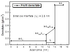
Fig. 2.1.1 MOS SiC/oxide profile and interface emphasis
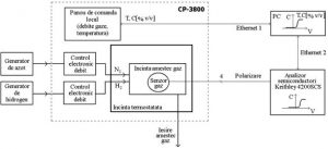
Fig. 2.3.1 SiC gas sensor electrical measurement and characterization system with temperature. Block Schematic
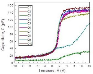
Fig. 2.4.1 C-V characteristics, measured on 10 SiC MOS capacitors

